(Hong Kong)

Product Summary
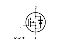
The SI2302DS is an N-channel enhancement mode field-effect transistor. Applications of the SI2302DS are battery management, high speed switch, low power DC to DC converter.
Parametrics
SI2302DS absolute maximum ratings: (1)VDS drain-source voltage (DC) Tj = 25 to 150 ℃: 20 V; (2)VGS gate-source voltage (DC): ±8 V; (3)ID drain current (DC) Tsp = 25 ℃; VGS = 4.5 V : 2.5 A; (4)Tsp = 70 ℃; VGS = 4.5 V: 2 A; (5)IDM peak drain current Tsp = 25 ℃; pulsed; tp ≦ 10 ms: 10 A; (6)Ptot total power dissipation Tsp = 25 ℃: 0.83 W; (7)Tstg storage temperature: -65 +150 ℃; (8)Tj operating junction temperature: -65 +150 ℃.
Features
SI2302DS features: (1)TrenchMOS technology; (2)Very fast switching; (3)Logic level compatible; (4)Subminiature surface mount package.
Diagrams
| Image | Part No | Mfg | Description |  |
Pricing (USD) |
Quantity | ||||||||||||
|---|---|---|---|---|---|---|---|---|---|---|---|---|---|---|---|---|---|---|
 |
 SI2302DS |
Other |
|
Data Sheet |
Negotiable |
|
||||||||||||
 |
SI2302DS,215 |
NXP Semiconductors |
MOSFET N-CH TRENCH 20V 2.5A |
Data Sheet |
|
|
||||||||||||
|
SI2302DS-T1 |
Vishay/Siliconix |
MOSFET 20V 2.8A 1.25 |
Data Sheet |
Negotiable |
|
||||||||||||