(Hong Kong)

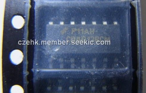
Product Summary
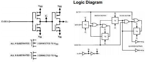
The CD4013BCM is a monolithic complementary MOS (CMOS) integrated circuit constructed with N- and P-channel enhancement mode transistors. Each flip-flop has independent data, set, reset, and clock inputs and "Q" and "Q" outputs. These devices can be used for shift register applications, and by connecting "Q" output to the data input, for counter and toggle applications. The logic level present at the "D" input is transferred to the Q output during the positive going transition of the clock pulse. Setting or resetting is independent of the clock and is accomplished by a high level on the set or reset line respectively.
Parametrics
CD4013BCM absolute maximum ratings: (1)DC Supply Voltage (VDD):-0.5VDC to + 18VDC; (2)Input Voltage(VIN):-0.5VDC to VDD + 0.5VDC; (3)Storage Temperature Range (TS) :-65°C to + 150°C; (4)Power Dissipation (PD):Dual-In-Line 700 mW;Small Outline 500 mW; (5)Lead Temperature (TL):(Soldering, 10 seconds) 260°C.
Features
CD4013BCM features: (1)Wide supply voltage range: 3.0V to 15V; (2)High noise immunity: 0.45 VDD(typ.); (3)Low power TTL: fan out of 2 driving 74L; compatibility: or 1 driving 74LS.
Diagrams
| Image | Part No | Mfg | Description |  |
Pricing (USD) |
Quantity | ||||
|---|---|---|---|---|---|---|---|---|---|---|
 |
 CD4013BCM |
Fairchild Semiconductor |
Flip Flops Dl D-Type Flip-Flop |
Data Sheet |
Negotiable |
|
||||
|
CD4013BCM_Q |
Fairchild Semiconductor |
Flip Flops Dl D-Type Flip-Flop |
Data Sheet |
Negotiable |
|
||||
|
CD4013BCMX |
Fairchild Semiconductor |
Flip Flops Dl D-Type Flip-Flop |
Data Sheet |
Negotiable |
|
||||